- Research
- Open access
- Published:
A novel FPGA-based test-bench framework for SDI stream verification
EURASIP Journal on Image and Video Processing volume 2020, Article number: 31 (2020)
Abstract
This paper presents a framework for complete simulation and verification of Serial Digital Interface (SDI) video using a verilog test-bench and geared toward FPGAs. This framework permits simulating the entire process: from test video signal generation to protocol verification in the FPGA which implements the Device Under Test (DUT). The novelty in the design is the combination of a customized test video signal generator with an implementation clone of DUT transceiver for in-depth protocol debugging. Identical input test patterns of the video protocol under test are generated and fed to DUT for verification. Thus, the model not only permits to evaluate the SDI transport layer but also validates the implementation at ultra low pixel level of the video format. This approach provides two advantages: cost saving in terms of additional lab test equipment and delivering all-in-one test solution to verify design and implementation. A practical implementation using a test example of a macroblock processing chain using SDI video interface shows the viability of the proposed framework for video protocol testing.
1 Introduction
Nowadays, there is a high demand for video processing applications such as media and entertainment, security and surveillance, and real-time streaming. This necessitates the development of new devices to handle the increasing demands in resolution and bandwidth. Emerging programmable System-on-Chip platforms combining Field Programmable Gate Arrays (FPGAs) with general purpose processors are suitable for running operating systems and to also accelerate algorithms at the hardware level. Hence, such platforms are a promising technology capable of providing the necessary power/performance trade-offs for emerging applications such as AI and video processing/coding amongst others. FPGAs can also support verification frameworks for other technologies, for example, it is possible to design an ASIC (Application Specific Integrated Circuit) device and perform its verification using an FPGA. However, due to the increasing complexity and size of such FPGA-based devices, the verification techniques become very important to validate the concreteness of a design and reduce the hardware errors and the time to market. Hence, the verification process represents a big challenge for design and verification engineers. This is further emphasized when considering that in real applications, the design needs to be verified with the operating conditions in mind which must include the communication, and synchronization with external interfaces and design correctness needs to be evaluated across various levels.
Current practices of analyzing designs involve incorporating a test-bench into the design to drive certain signal stimuli and compare the outputs of the design with the expected ones. The verification process is usually metric-driven, as for example coverage, that allows to measure the verification progress and determine when the design is ready. A brief metric description is presented in Section 2. These verification metrics have been improved and automatized during the last years by Ray Salemi and Mentor Graphics team that proposed the Universal Verification Methodology (UVM) [1, 2]. This method developed an automatic test-bench system able to perform high-level DUT verification using System Verilog. UVM goes further by providing mechanisms that allow constraints to be written as part of a test rather than embedded within dedicated verification components. This and other features of UVM facilitate the creating of reusable verification components. During the years, these techniques have been supported by Accellera System Initiative [3] and the advantages of its use are demonstrated in [4] using automotive examples. Verification methods are designed to be general and can be adapted for every testing scenario.
This work focuses on a framework dedicated to systems that use SDI interface to communicate and transmit data, geared toward video applications. Video formats are evolving fast with increasing resolutions, transmission rates, and video stream complexity [5]. SDI family is one of the most extended interfaces for transmission of uncompressed video between professional equipment [6]. As a consequence, there is a growing need for devices that can facilitate testing. However, new capabilities for video analysis usually represent a big cost in terms of developing testing devices, which are not always available since the most recent video standards are under continuous development. Due to the ever increasing resolutions in video standards and complexity, the need of faster devices has increased the use of FPGAs for video applications, as described in [7, 8]. This means that a verification method should be applied to allow testing the communication protocol and the device processing such as encoding, decoding, or filtering the signal. Often, the hardware analyzers and generators lack flexibility to modify the patterns for assessing the video test sequences, and they only offer the tests and formats available on the instrumentation, as is possible to check in [9, 10]. As a consequence, stream compatibility issues arise due to different video formats, components, or protocols; therefore, complete video analysis cannot be properly performed.
The main goal of this work is to investigate techniques to enhance verification for video processing. It improves the analysis capabilities of the internal functions of a device, including the operations involving data exchange with the external world through its communication protocols. Furthermore, it enables cost saving in terms of additional laboratory test equipment and it aims to deliver an all-in-one test solution to verify design and implementation.
The main advantages due to using this model are as follows:
-
It allows to insert video stream testing sequences into the DUT. It has the same behavior as if an external hardware signal generator is plugged through the HD-SDI physical interface.
-
It allows to compare the input and output stream of the DUT to verify its processing correctness. Throughout this comparison, it is possible to analyze the SDI transport layer, its protocol functionality and synchronization, and the video data components reaching pixel resolution.
-
It allows to check the DUT internal block delays; therefore, FPGA resources or external hardware are not required. Furthermore, it is not dependent on hardware manufacturers, simulators, and programming languages.
The verification methodology that is presented in this work can be applied to a numerous practical cases, especially where the data need to pass through a physical interface. In a specific video scenario, this method allows to test for example an encoder or a video filter in a professional production television environment, allowing to simulate not only the device but also its connections to the rest the equipment, simulating also the physical connection port and the communication protocol. We explain how to apply this framework in order to achieve a complete DUT observation, including simulation times, signal observability, chain delay, reduced FPGA resources occupation, and same signal captures. The solution is also compared where possible the state of art in order to evidence the improvements and main advantages provided by this framework especially on the observability of internal and external signals.
The remainder of this paper is organized as follows: In Section 2, the problem and main conditions are formulated. In Section 3, the verification framework is detailed. In Section 4, the validation experiments to show the model performance are described. In Section 5, results to show framework functionality are provided. Finally, conclusions are drawn in Section 7.
2 Background and related work
In this section, video analysis systems are described starting from the standard equipment up to the practical examples using FPGA test-benches.
The rapid increase resolution in video formats such as Ultra High Definition Television (UHDTV) is continuously setting for new requirements for information transport. Consequently, demand for techniques and testing/measurement equipment has also increased. A typical deployment for video measurements is shown in Fig. 1. This setting is composed of three main elements: (a) a signal generator that introduces a pattern signal test into the (b) Device Under Test (DUT) and (c) a wave monitor employed to visualize the signal characteristics to be analyzed. This common video testing setup allows signal analysis by means of several parameters such as eye diagram, jitter error, and cable losses. Further details can be found in [9, 11]. However, these parameters allow to assess the HD-SDI signal quality of measure only, because the wave monitor can analyze the physical layer, show the transport layer, but cannot debug it. This is an important drawback for more specific tests such as component analysis. The proposed framework is intended to permit SDI transport layer debug and data verification for all DUT components in a detailed manner (up to video components analysis).

SDI video equipment connected to the Device Under Test. The right side shows the main testing parameters that can be analyzed using a Hardware Wave Monitor
A more specific situation is to consider a development scenario where the DUT is implemented on an FPGA, which limits the clock frequency when compared to the frequency of the design in the real world. Performing a DUT data processing test with a physical wave monitor is not possible due to different clock rates between internal data processing and external data transmission. Additionally, wave monitor should be able to extract video data components and compare them with signal generator.
To validate hardware processing correctness, an internal signal analysis is required which can be performed using FPGA logic embedded analyzers (e.g., Vivado Logic Analyzer [12], Chipscope [13], or SignalTap [14]). However, video HD-SDI signal testing is not possible using internal FPGA logic analyzers because there is no interface that allows HD-SDI connection with embedded logic analyzers. A valuable alternative to face this problem is given by performing simulations before FPGA programming, but the standard test-bench can work only at DUT internal frequencies (e.g., 74.25 MHz or 148.5 MHz for HD video systems). FPGA test-bench cannot operate at SDI frequency (1.485 Ghz, 3 GHz,...) and is not suitable for SDI signal analysis.
An example of HD-SDI protocol is depicted in Fig. 2. It is composed of a Start of Active Video (SAV) which comprises four words that indicate the beginning of video components and an End of Active Video (EAV) which comprised four words indicating the end of video components. Both SAV and EAV headers are identified in the data stream by the following words: 3FFh,000h, and 000h. These words carry the timing information and avoid the use of traditional synchronization signals. The fourth word XYX contains signal information that permits to identify the following: (a) the SAV or the EAV header, (b) the field in case the video is interlaced, and (c) if data represent the vertical blanking or the video active. A digital line blanking ancillary data is sent after the EAV header that contains a two-word line number (LN0 and LN1), followed by a two-word CRC (CR0 and CR1). The CRC value is used to detect errors in the active video that follows the SAV. The information contained between EAV and SAV is called Horizontal Blanking. Figure 2 depicts the above described protocol; the n-1 words on the right part of the figure are called Active Video. It represents the luma and chroma pixel information which size depends of the video format. SDI protocol data rate is up to 12 Gbit/s[15]. Further details can be found in [6, 16].

HD-SDI components’ stream example
In video processing systems as the one shown in Fig. 1, DUT internal transceiver can match different data rates. Additionally, it also transforms the signal stream from serial to parallel and vice versa considering transmission or reception stage.
Performing HD-SDI hardware verification requires a generator able to introduce into the DUT a signal according to the video protocol standard. Moreover, checking the output sequence in order to guarantee data integrity in terms of processing and synchronization represents an important issue that test-benches do not solve without additional external hardware components.
A brief description about some verification metrics is as follows:
-
Functional coverage represents the measure of how much functionality of the design has been exercised by the verification environment.
-
Code coverage measures how much code is checked by the test-bench.
-
Constrained random testing provides a random stimulus as input, to push the DUT into interesting corner cases giving the means to reach coverage goals.
More details are available in [17]. Some test-benches are directly synthesized inside the FPGA. It represents an advantage in terms of test speed and signal data transfer rate between DUT and generator. However, it yields to waste FPGA resources which are critical for large-scale project development.
It could be used for video testing purposes; however, an external video signal transceiver for DUT complete simulation is required.
Alternatively, an FPGA synthesizable test-bench that allows fast execution times and chip observability for debugging is presented in [18]. Nonetheless, in addition to the need of adapting a video signal transceiver, the entire project is executed on the DUT physical memory. This leads to waste of FPGA resources.
Another approach to tackle this problem is proposed in [19]. The verification method compiles the test-bench on a computer. It connects internal blocks directly to a PCI-extended bus to introduce and receive signals to/from the DUT. However, HD-SDI implementation is not possible on the PCI-extended bus due to the demands for high data rates which are not possible under this configuration, because the PCI bus of the Altera Stratix II EP2S60F1020C4 used is a 33-MHz bus as detailed in [20], and cannot reach the HD-SDI data transfer rate. It could be possible using a new FPGA that uses a new PCI standard as described in [21].
A hybrid verification platform is presented in [22], where authors combine software simulation and hardware emulation. The experiment synthesizes a 32-bit DLX PCPU (pipelined CPU) on an Altera FPGA, an assembly program with a bug is run, and the FPGA internal behavior is recorded. The data is used to reconstruct the relevant segment of a simulation in ModelSIM [23] for debugging. This work allows to reduce the simulation times, and it permits to analyze the internal behavior of the FPGA and to debug its processing stage. However, in the SDI case, an external analysis is needed, because it allows to evaluate the correctness of video component insertion in the SDI protocol to be interchanged with other devices. This work does not consider this case.
The most similar work to the framework presented in this paper is [24], where a Phase Alternating Line (PAL) signal processing hardware and a test-bench are generated to accelerate hardware verification. However, interface debugging is not specified, while in case of video systems, it has to be considered not only the internal processing, but also the video data interchange over the interface. This is important because if the video data is not properly inserted, a synchronization issue will make the signal not understandable from the other devices (e.g., a television that does not receive a correct signal from a decoder cannot visualize it). Furthermore, this work cannot be used for HD-SDI verification because it uses analogical interfaces (S-Video and VGA) while HD-SDI is a digital interface; they also work with different data rates that are not compatible.
In references [18] to [24], some works about test-benches have been described; a resume and comparison with our work are presented in Table 1. In references [25] to [26], to emphasize the contribution of our proposed approach, some examples about its application will follow. It will be presented how our approach could help in issues related to the verification of complex video processing systems. A brief description about an existing approach will be followed with an explanation on how our proposed alternative can provide a more flexible and economic solution as a verification technique.
In the work [25], a low latency 3D hardware image rectification engine using FPGA and HD-SDI interface is presented. The authors have created a complex structure for verification and a Printed Circuit Board (PCB) for interface integration. In this case, the application of the proposed test-bench represents an advantage for the verification because it allows to compare the two streams during the simulation including HD-SDI interfaces. The simulation can provide important information before the creation of PCB and can prevent its redesign in case of FPGA hardware issues.
In [27], an architecture for exact computation of 2D Discrete Cosine Transform (DCT) 8×8 blocks on FPGA is presented. The verification is performed using Matlab. The Matlab workspace inputs data into the FPGA through the JTAG interface; the measured output is returned to the Matlab workspace for verification. In this case, to apply our test-bench avoids to migrate to Matlab workspace using FPGA simulation tools (i.e., [23, 28]) to validate the design. Another advantage is represented from the opportunity to simulate the design in a real environment where the signal is inputted through a video interface (not JTAG) and data is provided using a generator. Moreover, the complete chain can be verified through direct comparison between input and output video interfaces.
In the work [26], a real-time video stabilization system on FPGA is proposed. In this work, the authors use a PAL interface to interchange video data. A measurement environment is generated to evaluate the peak signal-to-noise ratio (PSNR) between the original video sequence and the stabilized video sequence. By means of the proposed verification, test-bench PAL interface can be simulated. Moreover, it permits upgrade to HD formats and the integration of digital video interfaces such as HD-SDI family. Furthermore, applying our test-bench allows to automatize the PSNR calculation and comparison between frames from both input and output for automatic assessment of the results.
In comparison with the other approaches presented in this section, our model allows to test the DUT using the same behavior than if an external hardware signal generator would be plugged through the HD-SDI physical interface. In contrast with the other approaches, it is possible to analyze the SDI video stream reaching pixel resolution and perform DUT verification analyzing internal block functionality and delays, without overhead in FPGA resources or external additional hardware. This framework flexibility is not dependent on hardware manufacturers, simulators, and programming languages, and allows the complete DUT verification due to its internal connection structure. This work presents a novel approach to the verification state of the art as it it improves the DUT observability. In Fact, it allows to check DUT internal signals by direct signal routing to the check block, without passing through an interface. This is a feature that is possible only during simulation.
3 Verification model
The framework structure is drawn on the right side of Fig. 3, and it is composed from many blocks. Block 1, block 2,... block N represent the processing chain of a design to analyze. It could be for example a video filter, an encoder, and a decoder. FPGA test-benches allow to analyze only these chain structures, where the test signal is introduced at the start of the processing chain and a check block at its end.

(Left) Standard test-bench model. (Right) Video test-bench framework with double transceiver system for SDI simulation. Blocks 1 to N represent the video processing chain
The chain is connected to a transceiver that communicates the input signal from physical layer, extracts the components that have to be processed from a protocol, and then provides them to the processing chain. After the processing chain has finished its tasks, it provides the data to the transceiver that will format them and send them to the physical output layer. The SDI family has a high data rate; it means that the input/output stage of transceiver works with high frequencies (more than 1 GHz for HD signals). A typical FPGA board has an internal clock of around 200 MHz, as shown in [29], that cannot reach the SDI clock frequency. The solution to match these different frequency rates is to transform signal from serial to parallel and work with multiple frequency (e.g., external serial signal at 1.485 GHz, internal parallel signal of 10 bits, and 148.5 MHz for HD-SDI).
In case of SDI video application, the transceiver has two functions:
-
In the input stage, it receives the signal from physical layer, extracts the video components from SDI stream, converts the signal from serial to parallel, and matches the different signal data rates (e.g., from 1.485 GHz to 148.5 MHz for HD-SDI) to make it suitable for the internal FPGA processing frequency rate.
-
In the output stage, it receives from the processing chain the video components as parallel signal at 148.5 MHz, encapsulates it in the SDI protocol converting the signal from parallel to serial, and provides it to the physical output layer (at 1.485 GHz for HD-SDI).
This is not possible to debug with standard FPGA tools (Signal tap by Altera, Chipscope by Xilinx) because they can only work with internal clock rates. To debug the complete signal, an analyzer is needed but it only offers some tests as already described in Section 2. In a simulation, it is possible to analyze the different frequency rates, but it is missing a test generator able to communicate with the DUT through the transceiver. At this point, the main idea of this work is to use a double transceiver structure shown on the right side of Fig. 3:
-
The first transceiver (called FPGA video signal transceiver on the right side of Fig. 3) represents the FPGA transceiver and allows to communicate with the processing chain using the SDI physical interface and protocol.
-
The second transceiver (called simulation video transceiver on the right side of Fig. 3) allows the communication between a custom test generator block with the rest of the structure, and to receive the processed signal to the signal check block over the SDI channel.
This double transceiver structure allows to simulate the entire DUT and connect a custom generator and a custom check block to test the DUT. It is important to remark that it is possible to use every custom routine for signal generating and signal checking that are not available in the physical analyzer and in normal test-benches. This structure can debug the internal DUT over the SDI interface and allows to test not only the functionalities of processing chain, but also the data integrity of video component and signal sync over the SDI interface. Moreover, conversely to standard hardware testing system shown in Fig. 1, the proposed framework can also access the response of every internal DUT component and drive its signal directly to the check block without inserting them in the rest of the processing chain through the transceivers. It results in a significant improvement of the testing observability. An example of a possible measure test is the DUT chain delay D that can be determined according to the following equation:
where m is the total number of internal DUT blocks, ccbk is the number of clock cycles required for k block processing, clk_freqk is the working clock frequency, and D is expressed in seconds.
Thanks to this flexible approach, it is possible to change the kind of test by just changing the code of generator and check blocks, and running another simulation. It also permits to automatize the testing routines or running a simulation with auto-checking routines. In the next section, the blocks employed for experiment validation are described.
4 Experimental validation methodology
4.1 Testing methodology
Video processing techniques such as video compression and video content analysis have been widely used in various applications. Most of them use a picture subdivision in squared areas called macroblocks. In detail, a macroblock is a square group of pixels used as elementary unit in video processing techniques; it could have a convenient dimensions depending on the application (e.g., 8×8,16×16,32×32). A typical application that uses macroblock subdivision is H.264 coding [30]. It represent a widely used standard in video applications. For this reason, many systems can interface with such coding schemes so it is necessary to guarantee correct and accurate verification process. The testing methodology developed in the DUT implements a video processing chain oriented to H.264 coding, focusing on macroblock processing. The main idea consists of a system that receives HD-SDI video stream, extracts the video lines, and organizes the data into macroblocks as shown in Fig. 4. At this point, the macroblocks will be ready for coding process. The experiment involves macroblock extraction and line restore, so the data will be sent to the output part of the chain that reorganizes macroblocks to create the video line. The proposed method is applied to the process already described for performing the verification. It uses a custom macroblock generator and a macroblock check module that permit to compare the two signals outside the DUT through the HD-SDI interface, allowing to evaluate the correctness of DUT internal processing chain.

Test-bench applied to a real case: the experiment validation model is ported on a Virtex-6 Xilinx FPGA
4.2 Global functional description
Figure 5 summarizes the functionality of the entire verification frame applied to the system; its description is as follows:

Complete chain functionality block diagram
The pattern generator creates the data that will be introduced into the transceiver that communicates with the DUT. The DUT transceiver receives the signal as a video line (in Fig. 4 and the components are depicted on the top right part as sequence line 0, line 1, and line 15). The video line is processed pixel per pixel until module Block RAM Buffer 256 to MB which stores the 16 lines and extracts macroblocks (as shown on the extreme right side of Fig. 4). The macroblocks are stored in the module Block RAM Buffer MB to Line which reconstructs the line and outputs the components to the rest of the chain. The lines pass through the transceivers until MB pattern check which permits to perform the comparison and verification with the pattern generation.
A great advantage offered by the proposed framework is the direct connection between each module of the DUT and the MB pattern check without entering into the transceiver.
4.3 Macroblock component extraction
Before a complete description of the system, it is important to introduce the test method employed to verify the correct extraction of the macroblock components. Following H.264 standard, to encode the video signal, a frame should be divided into macroblocks as detailed in references [30, 31]. In this experiment, a 16×16 matrix of pixels will be used as a macroblock dimension. For this reason, to create a macroblock sequence, it is necessary to process 16 video lines. To identify each component of the macroblocks, it is useful to have a pattern generator able to insert the data in a known order sequence. For this purpose, a custom frame generator is created to provide an ordered number sequence instead of video components. The principal benefit of this approach is the enumeration of each macroblock pixel by pixel. It allows to identify an eventual error in the process just checking if the output is respecting the enumeration order provided as input stream. The macroblock generator output is shown in Fig. 6 and consists in the generation of an ordered sequence of number repeated for 16 video lines (0 to 15) that allows to identify each macroblock with its number. An example of pattern is the following:
-
Line 0: 0000...1111...2222...3333... n−1,n−1,n−1,n−1
Fig. 6 
Custom generator for macroblock check. On the left side, the sorted component input line is shown. On the right side, the expected macroblock output is shown
-
Line 1: 0000...1111...2222...3333... n−1,n−1,n−1,n−1
-
.......................
-
Line 15: 0000...1111...2222...3333... n−1,n−1,n−1,n−1

where n−1 for 720p resolution (1280×720 pixels) is 1280/16−1=80−1=79, 80 corresponds to the number of macroblocks every 16 line, for a total of 3600 macroblocks per frame. Once this pattern is repeated, the DUT will be able to extract a macroblock of zeros, a macroblock of ones,...etc. If this process is performed n times, the entire frame will be generated (e.g., in 720p will be repeated n=720/16=45 times). It is possible to add markers for line pattern labeling. As an example, the line number can be labeled as follows:
-
aa0000...1111...2222...3333...aa n−1,n−1,n−1,n−1
The aforementioned process is depicted in Fig. 6. In this figure, an example of pattern generator output and macroblock composition is shown. The horizontal axis corresponds to the pixel arrangement, whereas the vertical axis represents the line numbers, for example:
-
MB0: line 0 to 15, pixels 0 to 15.
-
MB1: line 0 to 15, pixels 16 to 31.
-
.....................
-
MB n−1: line 0 to 15, pixels n−16 to n−1.
For a 720p format as shown in Fig. 7, the macroblock 79 will have line 0 to 15, pixels 1263 to 1279 position. The macroblock 3599, the last one in a frame, will have line 703 to 719, pixels 1263 to 1279 position.

Macroblock HD 720p frame subdivision example
4.4 Test-bench and detailed functional description
The DUT macroblock processing chain was developed and tested on a Xilinx ML605 evaluation board [32] featuring Virtex-6 XC6VLX240T-1FFG1156 FPGA [33]. Additionally, a Broadcast Connectivity FMC mezzanine card (CTXIL671) [34] was employed as physical interface to connect the HD-SDI signal to the ML605 board. As a proof of independence from the manufacturer, this framework can also be implemented in other FPGA company products. As an example, it could be developed on Altera FPGA using SDI MegaCore Functions IP [35]. Moreover, the software for FPGA programming is the ISE 14.7 design suite by Xilinx [36]. The computer used to run the simulations is based on an Intel(R) Core(TM) i7-2600 CPU @ 3.40GHz with 4GB of DIMM DDR3 RAM.
The DUT structure was developed according to the proposed verification framework depicted on the right part of Fig. 4. The figure represents how a real project is entirely simulated in a computer. On the left part of the figure, the MB pattern test generator shows the generator already described.
The functionality of the DUT blocks is detailed as follows:
-
The video signal transceiver is composed of two Xilinx Intellectual Property (IP) blocks: GTX transceiver and Triple-Rate SDI. The former allows to receive/transmit the HD-SDI protocol. In reception, the signal is acquired at 1485 Gbit/s, transformed from a serial to a parallel bus at 148.5 Mbit/s, matching the data rate. In the transmission stage, the transceiver performs the opposite operations. The latter permits to establish the communication between GTX transceiver and the rest of the chain. It decodes the GTX transceiver data coming from parallel bus into video components (lumas and chromas) and synchronization information (e.g., SAV, EAV, number of line). Conversely, in transmission, it encodes the processed video from chain and permits to add synchronization information. Further details on the Xilinx IPs mentioned can be found in [37].
-
The next blocks represent the processing chain. The data they process is the video components in pixels. The information of each pixel is represented using 10 bits in the HD-SDI stream. After that, it is normalized to 8 bit because it is more suitable for the internal FPGA memories and communication busses.
-
The next block of 10 to 8 bits reduces the output of the Triple-Rate SDI RX from 10 bits to 8; this allows to store luma and chromas into FPGA memories.
-
The block Buffer 8 to 256 of the DUT in Fig. 4 is a buffer that changes the 8-bit video signal component (Y, Cb, Cr) coming from the previous block into a bus of 256 bits. This size of bus has been chosen to attain a faster transportation of video components to the rest of project blocks.
-
The module Block RAM Buffer 256 to MB receives the 256-bit data and stores it in a memory with capacity to contain 16 video lines. Afterwards, it reads and reorganizes data in macroblocks of 16×16 pixels. As a result, every macroblock is provided at the output of this block under 8 component of 256 bits.
-
The module Block RAM Buffer MB to Line of Fig. 4 performs the opposite operation of the previous block. It receives the macroblocks, stores them in a FIFO, arranges video data in lines, and delivers it to the output.
-
The block Buffer 256 to 8 in Fig. 4 adjusts the signal from 256 bits to 8 and introduces it into the following block.
-
The block 8 to 10 in Fig. 4 adjusts the signal from 8 bits to 10 and introduces it into the Triple-Rate SDI TX block ready for output.
-
The test generator was previously described in Section 2.
The DUT is a real component that could be flashed into the FPGA whereas the test generator is not implemented on physical hardware since it is part of the simulation. In the next section, the results of simulations are provided. The simulations were performed using two different tools: the Xilinx ISim 14.7 [28] and ModelSIM SE 10.1C. [23] which remark flexibility of the proposed framework. Finally, two files with the test-bench code employed in this work are provided and can be downloaded from [38].
5 Experimental evaluation and results
In this section, the results of simulations performed according to the structure described in previous sections are presented. Full connectivity verification, video component, internal DUT observability, and time delays were verified. These results are shown in Figs. 8, 9, and 10 where three simulation captures summarize part of video sequences to display the most relevant features of this test. Three main sections to assess the framework performance follow next. Each section represents an experiment, in particular the A box in Fig. 8 refers to the macroblock extraction process from lines, and the B box in Fig. 9 represents the opposite operation where the macroblocks are reconverted into lines. Finally, the C Box in Fig. 10 is a test where the pattern generator is replaced by a standard bar generator. This replacement allows the simulation to validate the entire chain functionality. A complete description of every section is as follows.

The simulation screenshot represents the macroblock extraction process

The simulation screenshot corresponds to line reconstruction experiment

The simulation screenshot shows a complete chain experiment with bar generator
5.1 Macroblock extraction
In the experiment A of Fig. 8, the macroblocks are extracted from the lines. This experiment, as already depicted in the functional description in Section 4, includes the modules Buffer 8 to 256 and Block RAM Buffer 256 to MB of Fig. 4. The signals y_in8 and c_in8 in the box A1 correspond to the input of the module Buffer 8 to 256. Furthermore, the signals y_video_256 and c_video_256 in the box A2 represent the module Block RAM Buffer 256 to MB output. It is very important to remark that the input data is provided by the MB pattern test generator through the transceivers, but the analysis busses are connected directly to the MB pattern check block (allowing direct signal check, without passing through the transceivers); this is possible only in the simulation thanks to applying the proposed framework. The video lines arrive into the Block RAM Buffer 256 to MB until its buffer is full and therefore ready to extract the macroblocks. Once this buffer is full, it starts to output the macroblocks. This can be observed in the initial part of Fig 8, box A2 where both signals y_video_256 and c_video_256 are undefined (XXX...). Afterwards, it starts to output the macroblocks (0000... 0101...). This is clearly shown in the box A1 where macroblocks are delivered to output after the frame input is in line 16 (signal line_number = 10hex). The pixels in this simulation time are marked 02 according to the test-bench structure of Section 4.
5.2 Macroblock reverse conversion
In the experiment B of Fig. 9, the macroblocks are received and reconverted to lines. The conditions are the same than experiment A of Fig. 8, where the input signal is provided through the transceivers, but the internal verification busses are connected directly to the MB pattern check. This experiment analyzes the subsequent stage to the experiment A and includes the modules Block RAM Line Buffer MB to Line and Buffer 256 to 8 shown in Fig. 4. The signals y_video256 and c_video256 in the box B1 of the Fig 9 represent the input of module Block RAM Line Buffer MB to Line, while the signals y_out8 and c_out8 in the box B2, represent the output of the module Buffer 256 to 8. The capture of this simulation is taken in the instant after the previous module, in the experiment A is outputting the macroblocks. This is verified by the timing in the top part of boxes A and B. The modules of previous stage start to deliver macroblocks around 566,480 ns of simulation (box A2 signals y_video_256 and c_video_256); the data is available at the input of following stage at 571,350 ns, just 5000 ns later, the time needed by electronics to propagate data. This condition is confirmed by input signals (y_video256 and c_video256) of the module Block RAM Line Buffer MB to Line in box B1, where before 571,350 ns signals are undefined (XXX...) and after this moment are carrying the macroblocks. In box B2 just after a short delay (33.68 ns), it is possible to verify through the signals y_out8 and c_out8 that the line components are distributed. In this case, the delay is minimal because the main component of block Block RAM Line Buffer MB to Line is a FIFO, which can output data while the input is arriving [39].
5.3 Bar generator test
The complete chain is under test in the experiment C of Fig. 10. The input and output signals pass through the transceivers, simulating the same connection than the measurement system shown in Fig. 1 including transport layer debugging. The block MB pattern test generator has been replaced by a standard HD bar generator. This replacement allows to test the DUT in simulation in the same manner than using a real equipment. This experiment consists of the following steps:
-
1
Generate the HD-SDI signal bars
-
2
Receive this signal in the DUT transceiver
-
3
Extract macroblocks with the modules of experiment A of Fig. 8,
-
4
Recompose the line through the modules of experiment B of Fig. 9,
-
5
Output lines with transceiver and receive the signal in the module MB pattern check.
If this process is performed without errors by every component of the chain, in MB pattern check, the same signal created from the bar generator will arrive, with a delay accumulated during the chain processing. This experiment simulation is depicted in the box C of Fig. 10 and detailed as follows. Box C1 indicates if DUT and test generator are connected and that communication is established. It encloses two HD-SDI serial differential channels that correspond to the signal stream flow at 1485 Gbit/s between them. These signals represent the TX/RX HD-SDI transport layer connections illustrated in Fig. 3. No significant differences can be appreciated because of high data rate and channel codification.
Box C2 is composed of four data busses containing luma and chroma components. y_tx_check and c_tx_check are sent from signal generator to DUT. y_rx_check and c_rx_check represent the components that come out after processing stage and are routed to the check block. In this case, comparison between components yields to verify if there is any error in DUT processing modules. Additionally, synchronization data is inserted into these busses and can be also analyzed.
Box C3 contains a bus depicting the number line of each video frame. tx_line_num_check was routed from HD test generator to signal check block, whereas rx_line_num_check was routed from DUT to signal check block.
Marker C4 highlights the time delay. Simulation process permits to measure the delay evolution in the chain. Model granularity is guaranteed as delay can be observed for every single block. As a result, it is possible to evaluate the processing time for every DUT component, from pattern insertion to processed signal.
5.4 Time measurement and comparison
Table 2 describes a comparison of simulation time as a function of SMPTE SDI standard rates and video formats. The model was implemented in both mentioned tools (ISim vs ModelSIM). Tests consist of evaluating the time spent by the DUT to process a frame of different video resolutions.
The assessment metric for this test was minutes per frame processed. It can be seen that ModelSIM is around four times faster than ISim, probably because ISim does not scale well for larger designs [17]. Time employed for frame processing is longer due to the high data rate of interfaces (≈ Gbit/s) and large number of simultaneous signals (HD-SDI links increase in 3G and 6G format). It is important to remark that simulations were carried out using a i7-2600 CPU @ 3.40 GHz with 4 GB of RAM, which is not a powerful architecture for high-performance test purposes.
The third column of Table 2 shows the chain delay of DUT block processing. Simulation results are close to D times calculated using Eq. 1.
Table 3 represents an example of time calculation and measurement per component obtained for a 1080p signal simulation test. It allows to verify if every module respects its expected execution times. Additionally, there is a little difference between the calculated and measured time of modules Block Ram Line Buffer 256 to MB and Block Ram Line Buffer MB to Line. It depends on the internal component Block Ram which requires some extra clock cycles due to circuit propagation latency [39].
5.5 FPGA resource comparison
Table 4 represents a Xilinx ISE synthesis reports that summarize the FPGA resource utilization. On the one hand, the columns DUT with TB show the FPGA resource utilization in case the complete test-bench is synthesized, including signal generator, check block, and DUT. On the other hand, the columns DUT only show the FPGA resource utilization when only the DUT is synthesized. It only involves the transceiver and the chain to create macroblocks and restore them into lines (right part of Fig. 4). In the Logic Utilization column, the logic components are specified, while in the Used columns, the amount of used logic elements is detailed. The Available columns show the number of logic elements available in the FPGA. Finally, the Utilization columns detail the percentage of logic elements used by the design. Comparing the Utilization columns of both images, it is possible to verify that the design including the test-bench needs more FPGA resources than the design with DUT only. An exception is represented by BUFG/BUFGCTRLs, since these are the input/output buffers, and the DUT only design requires more buffers to communicate with the output. From this example, it can be observed that the proposed framework is less restrictive in terms of FPGA resources, which can be useful for projects where FPGA resource utilization is critical.
5.6 Real case test-bench evaluation
In this section, the test-bench is applied to a real case to detect and solve an issue in a video processing application. As described in the previous sections (4), this method has been developed for assessing macroblock processing, for applications that utilize H.264 encoding. DCT-based coding algorithms such as H.264 divide the video frames into macroblocks. Within the encoder implementation, the input process needs to provide the macroblocks. This process reads the lines from the input frames and arranges the video components into the mentioned squared pixel structures. For debugging purposes, the same lines should be reconstructed from the H.264 encoder and then provided back. Two processing modules are needed to perform the H.264 encoding: the input chain (creating macroblocks from lines) and the output chain (extracting the video lines from the encoded macroblocks). The real test consists of implementing and testing the input and the output chain depicted in the DUT of Fig. 4, on Xilinx ML605 evaluation board [32] with a Virtex-6 XC6VLX240T-1FFG1156 FPGA [33]. The interface used is a Broadcast Connectivity FMC mezzanine card (CTXIL671) [34] that allows connecting the FPGA with SDI equipment. This configuration enables us to test the proposed experiment with the real hardware and compare its analysis capabilities with our test-bench. In fact, the FPGA is connected with real equipment such as a signal generator and a monitor. Figure 11 depicts the equipment connections to perform the test. The signal generator used is the BrightEye 57 from Ensemble design [40] that inputs the signal into the FPGA through a HD-SDI interface. The FPGA contains all the implemented modules including the input and output chains and provides output signal to the HD-SDI distributor. At this point, the signal is visualized on a BlackMagic SmartView monitor [41] and at the same time to a Omnitek HD-SDI video analyzer [42]. This permits to visually inspect the video on the screen and at the same time to analyze it using the Omnitek debug tool. The test signal chosen is a “Pathological pattern signal,” a special sequence that is capable to stress the SDI format especially used for equipment test. In fact, a conventional video signal could generate errors but may be transparent or very difficult to identify, while with the pathological signal, if there are some implementation bugs (both at hardware or software level) in the device, they will be noticeable and can be easily detected. More information about the pathological pattern signal is available in [43]. The test is carried out using a 1O80p25 resolution format. Once the test signal is introduced to the FPGA, the system starts generating some video artifacts, as is possible to see on the left part of Fig. 13, and a debugging stage is executed. The Omnitek analyzer provides the following information as shown in Fig. 12:
-
Do not recognize 1080p format
Fig. 11 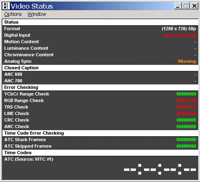
Output from the Omnitek video analyzer
Fig. 12 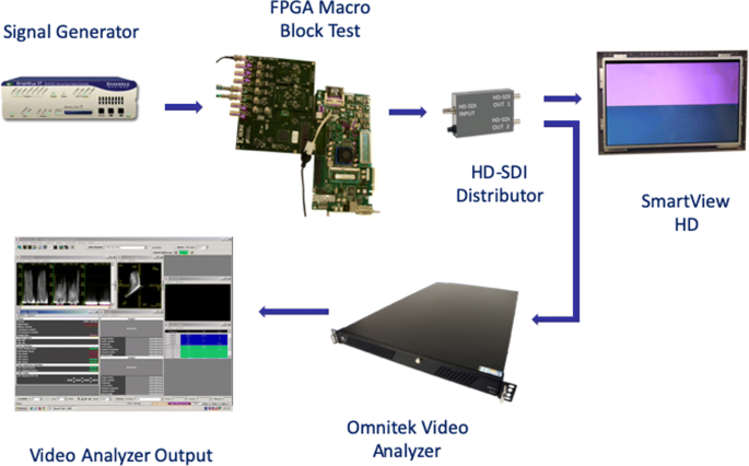
System connection to test the macroblock FPGA input/output chain
Fig. 13 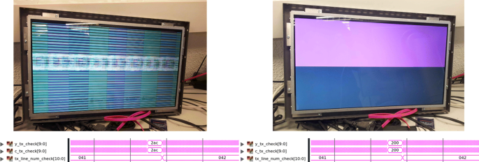
The test-bench is applied to solve a real case: a vertical synchronization issue
-
RGB color space error
-
Synchronization TRS error
-
Line check error


Unfortunately, the information is not sufficient to solve the issue. Furthermore, it does not specify where the errors occur. It remains unknown whether the error proceeds from the input stage or the output stage, or the process is failing to extract or recompose the macroblocks. Furthermore, it is not possible to perform a deep debugging with the Omnitek or other standard analyzers. At this point, the simulation presented in this work could provide a better internal observability. A pathological signal generator is introduced in the simulation and is possible to route all desired signals to the signal check block. After debugging, the issue is discovered in the output chain before the GTX transceiver. The vertical synchronization issue was generated by a wrong video component counting before the GTX transceiver. In fact, the wrong SAV code was generated and this resulted in blanking video components being mixed with active video components. As the issue propagates, a video artifact was generated as is also displayed in the monitor. Figure 13 is composed of the photos of the monitor output and by a small captures of the simulations. On the left side, the monitor shows the graphical artifact and its respective simulation. The analysis contains the output video components and the output line number. The code 2ac shown on the video components represents the SAV of the line 41 while the line 42 is going to be outputted by the GTX transceiver. On the right side of Fig. 13, the issue has been solved and the system sends to the output the right number of video components and the right synchronization code 200. More information about vertical HD-SDI synchronization codes is available in [16]. This experiment clearly shows that the proposed test-bench can provide finer testing over existing approached thus enabling easier debugging for H.264 applications.
6 Discussion
To the best of our knowledge, our work, compared to previous works, facilitates the verification of the design implementation and enables cost saving in terms of additional testing equipment. The effectiveness of our work has been demonstrated in Section 5.6 where our the test-bench has been compared with a professional video analyzer by Omnitek. Through experimentation, it was observed that existing approaches lack internal debug capabilities that our solution can provide in order to debug video applications. In comparison with other works [18, 19, 24], we also provide additional capabilities. We introduce test signals within the double transceiver architecture (to encode/decode video stream) making our solution capable of analyzing a complete solution.
Furthermore, other works employ different interfaces (PCI [19], RS232, USB, S-Video[24]) to input/debug data, which means that a previous signal transformation stage should be introduced to enable HD-SDI format analysis. As a result, it is not possible to analyze complete HD-SDI stream because information such as synchronization and number of line is lost. Moreover, in [24], an observation window is analyzed, whereas this work allows to debug the complete data flow (all the video frames desired). Referenced works do not allow direct comparison of input and output video data stream, neither are compatible with HD video formats. In addition, they do not provide results about simulation time nor data of interest comparable with our presented work.
Observability improvement of the proposed method is demonstrated since this information is internal and there is no accessibility from outside the DUT. Model flexibility allows to modify the bus observed at the check block by routing the signal/bus desired.
7 Conclusion
In this paper, a novel test-bench framework for SDI video systems has been presented. It permits to perform complete DUT verification in the same manner as a physical flexible hardware in cases where the latter is not available. It is especially suitable for deployment in verification environments that exhibit limited resources for DUT occupation and require flexibility in terms of signal generators and check blocks. In addition, the proposed framework is also applicable in cases where the DUT is only accessible through a protocol and/or a transceiver. As shown through the experimental evaluation on an FPGA, the verification methodology is applicable to real and practical use-cases and can be used to improve the simulation and verification process for engineers and hardware designers. Finally, this work has demonstrated that the inclusion of transceivers in SDI testing applications is indeed possible contrary to claims provided by manufacturers in design guides [44, 45]. As future work, it is interesting to test this framework with other interfaces and protocols (for example, HDMI in video systems or others such as Ethernet and USB). Another interesting point is the integration with UVM [1, 2] methodology to improve the automatic testing routines.
Availability of data and materials
The test-bench code employed in this work is available in [38], Data sharing is not applicable to this article as no datasets were generated during the current study.
Change history
22 October 2020
An amendment to this paper has been published and can be accessed via the original article.
Abbreviations
- DUT:
-
Device Under Test
- SDI:
-
Serial Digital Interface
- HD:
-
High definition
- PAL:
-
Phase Alternating Line
- FPGA:
-
Field Programmable Gate Array
- SAV:
-
Start of Active Video
- EAV:
-
End of Active Video
- IP:
-
Intellectual property
- GTX Tranceiver:
-
Video Tranceiver Xilinx primitive
- Triple-Rate SDI:
-
Xilinx IP that provides receiver and transmitter interfaces for the SMPTE 259M 292M 425M standards
- SMPTE:
-
Society of Motion Picture and Television Engineers timecode
- MB:
-
Macroblock
- CRC:
-
Cyclic Redundancy Check
- FIFO:
-
First In, First Out
- Block Ram:
-
Configurable memory module
References
R. Salemi, FPGA Simulation: A Complete Step-by-Step Guide (Boston Light Press, Boston, 2009).
R. Salemi, in Design & Test of Computers, IEEE vol. 26, no. 6 pp. 84-94, Nov.-Dec 2009. The uvm primer: a step-by-step introduction to the universal verification methodology (Boston, 2013). ISBN: 0974164933, 9780974164939.
G. Moretti, in IEEE Design & Test, vol. 34. Accellera’s support for ESL verification and stimulus reuse, pp. 69–75. https://doi.org/10.1109/MDAT.2016.2642898.
M. Barnasconi, et al., UVM-SystemC-AMS framework for system-level verification and validation of automotive use cases in. IEEE Des. Test. 32(6), 76–86 (2015).
DigiTAG and Analysis Mason, Roadmap for the Evolution of DTT - A Bright Future for TV. Brussels: DigiTAG (2014).
SMPTE 292M-1998. Television - Bit-Serial Digital Interface for High Definition Television Systems.
J. Fowers, G. Brown, P. Cooke, G. Stitt, in Proceedings of the ACM/SIGDA international symposium on Field Programmable Gate Arrays - FPGA ’12. A performance and energy comparison of FPGAs, GPUs, and multicores for sliding-window applications (ACM Press, 2012). https://doi.org/10.1145/2145694.2145704.
P. Sjövall, V. Viitamäki, J. Vanne, T. D. Hämäläinen, A. Kulmala, FPGA-powered 4K120p HEVC intra encoder (IEEE, 2018). https://doi.org/10.1109/iscas.2018.8351873.
WFM, 8200 and WFM8300 Waveform Monitors User Manual, Tektronix (2012).
Signal Generator. https://questtel.com/unit/3g-sdi-pattern-generator/. Accessed 24 Nov 2014.
Werner Klütsch, Winfried Schultz, Quality control and measurement in HD, EBU / IRT HDTV Brief. Geneva Tektronix. Tektronix. 22:, 1–50 (2005).
UG, 908 programming and debugging. https://www.xilinx.com/support/documentation/sw_manuals/xilinx2016_1/ug908-vivado-programming-debugging.pdf. Accessed 22 Sept 2014.
UG, 750 - ISE tutorial: using Xilinx ChipScope Pro ILA Core with project navigator to debug FPGA application. https://www.xilinx.com/support/documentation/sw_manuals/xilinx14_7/ug750.pdf. Accessed 21 Oct 2014.
Using SignalTap II Embedded Logic Analyzers in SOPC Builder Systems. https://www.altera.com/en_US/pdfs/literature/an/an323.pdf. Accessed 29 Sept 2014.
ST 2082-1:2015 Am1, in ST 2082-1:2015 Am1:2016. SMPTE Amendment - 12 Gb/s Signal/Data Serial Interface - Electrical - Amendment 1, (2016), pp. 1–2. https://doi.org/10.5594/SMPTE.ST2082-1.2015Am1.2016.
Guy Lewis, Michael Waidson, A Guide to standard and high-definition digital video measurements. Tektronix (2001).
E. Stavinov, 100 Power Tips for FPGA Designers (CreateSpace, Scotts Valley, 2011). ISBN 1461186293, 9781461186298.
I. Mavroidis, I. Mavroidis, I. Papaefstathiou, Accelerating emulation and providing full chip observability and controllability. IEEE Des. Test Comput.26(6), 84–94 (2009). https://doi.org/10.1109/mdt.2009.136.
X. Cheng, A. W. Ruan, Y. B. Liao, P. Li, H. C. Huang, in 2010 International Conference on Communications, Circuits and Systems (ICCCAS). A run-time RTL debugging methodology for FPGA-based co-simulation (IEEE. https://doi.org/10.1109/icccas.2010.5581847.
Handbook Stratix II Device Volume 1. https://www.intel.com/content/dam/www/programmable/us/en/pdfs/literature/hb/stx2/stratix2_handbook.pdf. Accessed 14 Nov 2014.
Streaming multichannel uncompressed video in the broadcast environment. https://www.intel.com/content/dam/www/programmable/us/en/pdfs/literature/wp/wp-01121-multichannel-uncompressed.pdf. Accessed 1 Dec 2014.
C. L. Chuang, W. H. Cheng, D. J. Lu, C. N. J. Liu, Hybrid approach to faster functional verification with full visibility. IEEE Des. Test Comput.24(2), 154–162 (2007). https://doi.org/10.1109/mdt.2007.46.
Mentor Graphics debug and analysis environment. http://www.mentor.com/products/fv/modelsim/. Accessed 24 Nov 2014.
A Trost, A žemva, in 2012 Proceedings of the 35th International Convention MIPRO. Verification structures for design of video processing circuitsOpatija, 2012), pp. 222–227.
H. Hübert, B. Stabernack, F. Zilly, Architecture of a low latency image rectification engine for stereoscopic 3-D HDTV processing. IEEE Trans. Circ. Syst. Video Technol.23(5), 813–822 (2013).
J. Li, T. Xu, K. Zhang, in IEEE Transactions on Circuits and Systems for Video Technology, vol. 27, no. 4,Real-time feature-based video stabilization on FPGA, pp. 907–919. https://doi.org/10.1109/TCSVT.2016.2515238.
A. Edirisuriya, A. Madanayake, R. J. Cintra, V. S. Dimitrov, N. Rajapaksha, A single-channel architecture for algebraic integer-based 8X8 2-D DCT computation. IEEE Trans. Circ. Syst. Video Technol.23(12), 2083–2089 (2013).
ISim Xilinx simulator. http://www.xilinx.com/tools/isim.htm. Accessed 21 Oct 2014.
Xilinx Virtex-7 FPGA Board specification. https://www.xilinx.com/products/boards-and-kits/ek-v7-vc707-g.html#hardware. Accessed 29 Sept 2014.
ITU-T Rec. H.264, Advanced video coding for generic audiovisual services (2016). https://www.itu.int/rec/T-REC-H.264-201610-S/en. Accessed 14 Jan 2015.
ITU-T Rec. H.265, High efficiency video coding (2016). https://www.itu.int/rec/T-REC-H.265. Accessed 14 Nov 2014.
Virtex-6 FPGA ML605 Evaluation Kit. https://www.xilinx.com/products/boards-and-kits/ek-v6-ml605-g.html. Accessed 26 Jan 2015.
Virtex-6 Family Overview. https://www.xilinx.com/support/documentation/data_sheets/ds150.pdf. Accessed 26 Jan 2015.
CTXIL, 671 Board. http://www.cook-tech.com/ctxil671.php?OrderOnline=More+Info&TICOM_AUTHLEVEL=3&TICOM_VALIDATE. _INPUT=1. Accessed 26 Jan 2015.
Altera Video transceiver IP. https://www.altera.com/products/intellectual-property/ip/interface-protocols/m-alt-sdi.html. Accessed 14 Jan 2015.
ISE Design Suite. https://www.xilinx.com/products/design-tools/ise-design-suite.html. Accessed 18 Sept 2014.
Xilinx Application with Video transceiver IP. http://www.xilinx.com/support/documentation/application_notes/xapp1075_V6GTX_TripleRateSDI.pdf. Accessed 29 Sept 2014.
Downlodable testbench Code. https://github.com/gic81/verilogtestbench. Accessed 29 Sept 2014.
Virtex-6 FPGA Memory Resources. https://www.xilinx.com/support/documentation/user_guides/ug363.pdf. Accessed 14 Jan 2015.
BrightEye 57 3G/HD/SD/Analog Test Signal and Sync Pulse Generator. https://www.ensembledesigns.com/products/brighteye/be57. Accessed 30 Jan 2015.
Blackmagic Smartview HD. https://www.blackmagicdesign.com/uk/products/smartview4k/techspecs/W-HDL-09. Accessed 18 Feb 2015.
Omnitek HD-SDI Video Analyzer. https://www.intel.com/content/www/us/en/design/support-and-training/omnitek-test-and-measurement.html. Accessed 4 Mar 2015.
Physical Layer Testing of 3G-SDI and HD-SDI Serial Digital Signals. https://download.tek.com/document/Physical-Layer-Testing-3G-SDI-HD-SDI-Serial-Digital-Signals_AppNote_25W-19525-3.pdf. Accessed 4 Mar 2015.
SMPTE UHD-SDI v1.0 - LogiCORE IP Product Guide. https://www.xilinx.com/support/documentation/ip_documentation/v_smpte_uhdsdi/v1_0/pg205-v-smpte-uhdsdi.pdf. Accessed 1 Apr 2015.
XAP, 1249 - Implementing SMPTE SDI Interfaces with 7 Series GTX Transceivers. https://www.xilinx.com/support/documentation/application_notes/xapp1249-smpte-sdi-interfaces-7series-gtx-transceivers.pdf. Accessed 25 Sept 2015.
Acknowledgements
The authors thank the editor and reviewers for their helpful comments and suggestions.
Funding
Not applicable.
Author information
Authors and Affiliations
Contributions
All authors take part in the discussion of the work described in this paper. The author read and approved the final manuscript.
Corresponding author
Ethics declarations
Competing interests
The authors declare that they have no competing interests.
Additional information
Publisher’s Note
Springer Nature remains neutral with regard to jurisdictional claims in published maps and institutional affiliations.
The original version of this article was revised: the body text was corrected as well as Figures 11 and 12 were rightly inverted and adjusted.
Rights and permissions
, corrected publication 2020 Open Access This article is licensed under a Creative Commons Attribution 4.0 International License, which permits use, sharing, adaptation, distribution and reproduction in any medium or format, as long as you give appropriate credit to the original author(s) and the source, provide a link to the Creative Commons licence, and indicate if changes were made. The images or other third party material in this article are included in the article’s Creative Commons licence, unless indicated otherwise in a credit line to the material. If material is not included in the article’s Creative Commons licence and your intended use is not permitted by statutory regulation or exceeds the permitted use, you will need to obtain permission directly from the copyright holder. To view a copy of this licence, visit http://creativecommons.org/licenses/by/4.0/.
About this article

Cite this article
Conti, G., Kyrkou, C., Theocharides, T. et al. A novel FPGA-based test-bench framework for SDI stream verification. J Image Video Proc. 2020, 31 (2020). https://doi.org/10.1186/s13640-020-00515-5
Received:
Accepted:
Published:
DOI: https://doi.org/10.1186/s13640-020-00515-5